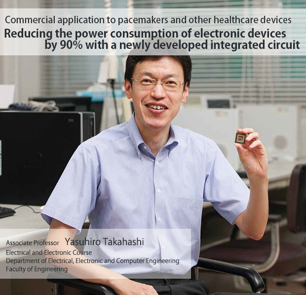
Reducing the power consumption of electronic devices by 90% with a newly developed integrated circuit
Reducing power consumption by directly using AC voltage
In the world todays, integrated circuits (ICs) are embedded in all kinds of electric and electronic devices, such as refrigerators, PCs, and mobile phones. Electric energy supplied from a power source activates many transistors (switches) inside to serve as the brain that controls those devices.
Current ICs are operated with DC voltage that is converted from AC supply voltage, but the conversion process using an AC adaptor or battery can also consume power. To attempt to reduce such power loss, I have been researching the design of an IC called the "adiabatic logic circuit." As a result, I was able to build a prototype that could be installed in a healthcare product. This IC is 155 µm × 172 µm in size, or about the thickness of a human hair.
*µm: Unit of length equal to 0.001 mm.
An adiabatic logic circuit is able to use AC voltage as its power source without converting it to DC voltage. In the IC system, the circuit is operated by using digital domain signals that is 0 and 1. Up until today, this calculation process has wasted energy (or electric power) needlessly and generated heat. However, as the name "adiabatic" implies, the new circuit does not waste energy, but rather recovers part of the power as its supply power, thus reducing power consumption.
Inspiration to effectively combining two AC voltages
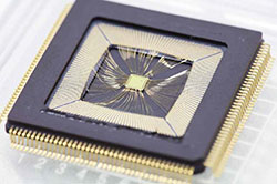
human hair is embedded in a square measuring
2.4 mm × 2.4 mm located in the center.
(Integrated circuit was produced by a manufacturer
for study purposes)
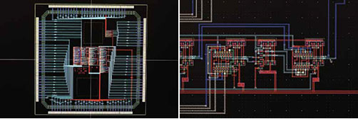
Students in the laboratory made these drawings on a computer, and a manufacturer produced integrated
circuits based on the drawings. The transistors inside the circuit are made of various materials with or
without conductivity. The red line denotes metal that conducts electricity; the green line denotes
silicon that does not conduct electricity. The white line is about 1/100 of the thickness of a human hair.
The students also drew such ultra-thin lines one by one. It can take about two months to complete one
drawing. In the testing process, electric current is provided to the circuit to verify its operation
while switching the transistors.
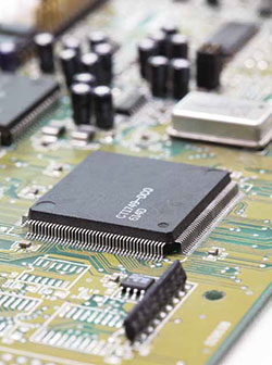
are used in a general CPU that conducts a variety
of calculation processes by switching the
transistors to operate PC.
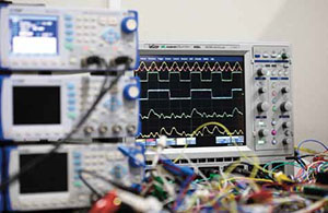
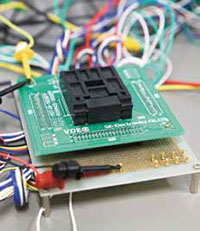
study on the adiabatic logic circuit. Six units are
currently used, but in the future the unit will also be
downsized and integrated into the integrated circuit.
My proposed adiabatic logic circuit is operated with the use of two AC voltages (sine waves) as its power source. A certain manufacturer was researching whether to introduce this logic circuit to the CPU of a PC, in order to reduce energy consumption. But CPU operating speeds at that time had already reached a high frequency level of 500 MHz, thereby rendering the circuit not advantageous for such purpose. The reason is that, as I found later, the adiabatic logic circuit saves energy more effectively by using two waveforms of gentle fluctuations and by matching them with the timing of calculation. The faster the speed, the more difficult it becomes to match the signal timing. I consequently came to realize that this circuit could be only applied to healthcare devices or wristwatches that do not need the circuit to operate at such high speed. These devices fully operate even at a speed of about 1 MHz, and thus present very good possibilities for utilizing in the circuit.
*CPU...central processing unit of a computer or similar device, with arithmetic processing function that controls various components and processes data
When I was a Ph.D. student, my supervisor told me that "inspiration comes to you when you are taking a bath, in bed or driving a car," and that is what happened to me. I just suddenly came up with the idea of using two AC waveforms and the possible application to healthcare products.
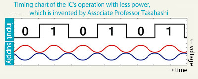
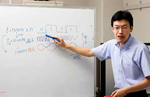
by combining two AC voltages. To reduce the loss of electric energy by
synchronizing the operating signals with slowly raising or lowering the supply
voltage. (See the figure below) The study continues for realizing commercial
application within five years.
At this point, our laboratory has been designed an IC that can reduce power consumption to one-tenth of the current level. Eventually, I hope to achieve a reduction to one-thousandth power dissipation. This requires further power saving of the power source generation unit that generates two sine waves, as well as the development of an auto correction circuit that matches the timing of waveforms. My final goal is to integrate these peripheral circuits into one small chip. I believe that if I could ever realize this, it would surely improve the energy saving capacity of any type of electronic devices used in our society.
Medical and healthcare products that use electric current generated by humans
I am thinking about medical or sports support devices as realistic application possibilities for the adiabatic logic circuit. Such medical devices include the pacemaker. Its battery life is generally 8 to 10 years, but could be even 10 times longer if we utilize the adiabatic logic circuit. Each heartbeat generates very weak AC of a few millivolts. If we can use that current for operating the circuit, there will be no need for replacement surgery as long as the person remains alive.
The circuit can also be applied to sports-related products. By embedding the circuit in the soles of shoes, running speed and other variables could be measured using the electric current generated by the vibration of running.
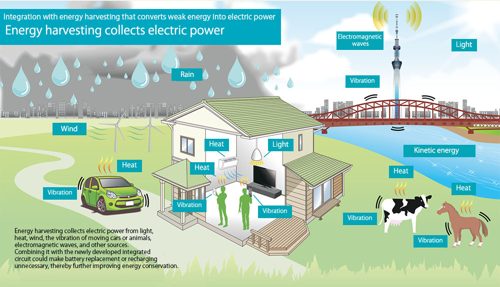
Working on energy harvesting that uses environmental energy as well
I am also studying "energy harvesting" or the technology that harvests and converts feeble energy generated in the natural environment into electric power, similar to the current generated by human movement as mentioned earlier. DC offers the advantage of being storable in a battery, but the disadvantage of limited service life. In our environment, there are various energy sources such as wind, light, heat, water, vibration, and electromagnetic waves. If we could collect AC supply from these energy sources and use it directly as it is, we would be able to realize much more extensive energy savings than being achieved today.
For example, we can embed the circuit in car tires to constantly monitor the air pressure or detect punctures. All we need to do is just put the circuit in the tire and operate it by using AC generated from vibration while the car is moving. If we apply it to a smart phone or PC, recharging will become almost unnecessary because energy is supplied whenever the device is moved. Solar batteries would also have higher generating capacity when integrated with energy harvesting by means of an embedded circuit.
| Expected fields of possible application |
|---|
| ・Healthcare products (Pacemakers, etc.) ・Measuring instruments for sports activity ・IC pass for train ・Smart phones ・PCs, etc. |
I feel that the Chubu region where Gifu University is located offers a fine environment for joint research projects as a number of automotive, aeronautical and other manufacturers are based here, and keenly working on the application of these ICs. I would like to promote the study of manufacturing that contributes to our society by further improving energy conservation in cooperation with the laboratories of other fields, both inside and outside our university.

Students involved in research
I want to contribute to people's lives through the study of a sub-threshold circuit that operates with ultra-low voltage.
I didn't know about the adiabatic logic circuit until I joined the lab, but became deeply interested in it after I came to understand the theory of saving power by slowly changing the voltage. I am now conducting research on further reductions in power consumption by combining the adiabatic logic circuit with a sub-threshold circuit that operates with voltage far lower than that used for conventional integrated circuits. In some cases, I have to make calculations for a week or so, just to reconfirm that this combination results in greater power savings. But I will feel a special sense of accomplishment when I am finally able to successfully prove it and rationally explain it with the calculation results. This is the ultimate pleasure of this study.
If this new circuit is implemented, it will enable substantial power savings for a wide diversity of electric and electronic devices, such as PCs and mobile phones, not to mention pacemakers. A longer lasting battery will reduce the need for heart surgeries, and the PCs and our phones will be much more useful. I believe this new circuit will surely improve people's lives. Therefore, I am determined to continue promoting the current study at this university even after completing my current course, in order to realize that new circuit as soon as possible.

I would like to further reduce power consumption through a study on combining the adiabatic logic circuit with three-dimensionally structured transistors, and then achieve commercialization of this design.
I became interested in this field because my father is also engaged in work related to integrated circuits, and then chose this lab to work in. At the moment, I am studying a type of integrated circuit wherein the adiabatic logic circuit is combined with three-dimensionally structured transistors called "FinFET."
Transistors are usually arranged in a plane structure, but applying a spatial structure and the adiabatic logic circuit could reduce power loss and further reduce power consumption, respectively. In order to find out how much power could be saved, we simulated the application of conventional DC as well as AC by connecting the adiabatic logic circuit to an integrated circuit in which transistors are structured three-dimensionally. The results plotted on a chart suggest that energy consumption could even be reduced to a maximum of one-thousandth of the current level. The more complex the circuit, the longer it takes to complete the simulation. And although it may take a few days just to create one chart, I feel rewarded when actually seeing the positive results of our study.
It is my wish to utilize the study results for product development in the healthcare or medical field, hopefully as a staff member of a leading company's R&D division. I want to contribute to our society by making such products available to as many people who need them as we can.